Technion FTA
"Nanophotonics for Advanced Light Detection"
Focal Technological Area – Focal technology areas (FTAs) constitute a cornerstone of the present phase of the Nanoscience and Technology National Program. The FTAs facilitate development of new nano-technologies and serve as engines for technology transfer to industry and for commercialization. The FTA program started on January 2012 in the six participating institutions, corresponding to the onset of the second nanoscience national program.
The Technion FTA- 'Nanophotonics for Detection and Sensing' aims at providing the science and technologies to overcome the gap between the research and industrial applicability in the field of advanced detection, probing, inspection, and sensing. Exploiting the strength of the Technion in photonics materials, device and systems and the large photonic industry in Israel, the aim is to provide solutions to the relevant defense as well as commercial industries. In the framework of the "Nanophotonics for Detection and Sensing", The FTA enables Technion to add to its infrastructure a major tool – a state of the art electron beam writing system.
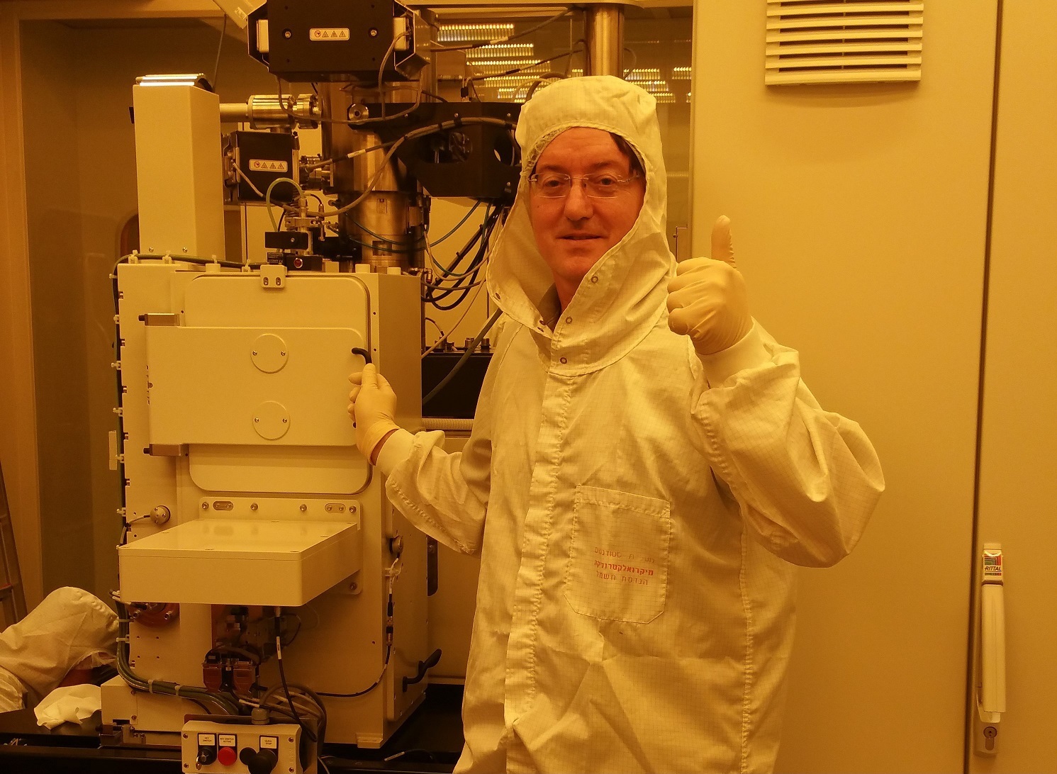
The EBL - one of the most advanced electron beam lithography (EBL) tools in the world the EBPG5200 of Raith, arrived at the Technion at the end of August 2015, and is now installed in the Micro/Nano Electronics Center. This EBL is capable of preparing few tens of atoms wide patterns (few nanometers) at very high rates on large wafer areas.
This unprecedented capability is promoting the Technion nanofabrication to the level exhibited only in very few advanced nanotechnology centers in the world. This tool will open new avenues in the realization of novel extreme nano electronics, photonics, devices, metamaterials for future low power computing, communications and biotechnology.
Furthermore - The new EBL is a fully automatic system - and will save more than 90% of the time used today for operating older systems - allowing for more creative-thinking time for the young researchers. The large wafer capability and high throughput are critical enablers for academia-industry collaborations - a key goal for the Technion nano-activity. In addition, the Technion researchers will collaborate with the manufacturer to enhance further the tool capability e.g. to write nanopatterns on non-flat (curved) surfaces.
To enable this very delicate operation - the Technion invested in preparing a special facility comprised of a clean laboratory with temperature stabilized much better than 1/10 of a degree, while the EBL tool is hooked to tens of tons concrete basis which is floating on compressed air to mitigate environmental vibrations.